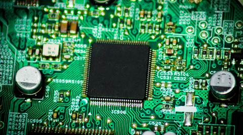
A research team led by US Department of Energy’s Lawrence Berkeley National Laboratory has created the world’s smallest transistor with a working one-nanometre gate.
In a study published in the journal Science, the researchers described the novel transistor made with a new combination of materials that is even smaller than the smallest possible silicon-based transistor.
“We made the smallest transistor reported to date,” said lead researcher Ali Javey from Lawrence Berkeley National Laboratory.
Instead of using silicon, the researchers built their prototype device with a class of semiconductor materials called transition metal dichalcogenides, or TMDs.
Specifically, their experimental device structure used molybdenum disulfide for the channel material and a single-walled carbon nanotube for the gate.
“Silicon transistors are approaching their size limit,” said one of the study authors, Moon Kim, Professor at The University of Texas at Dallas.
“Our research provides new insight into the feasibility to go beyond the ultimate scaling limit of silicon-based transistor technology,” Kim explained.
As current flows through a transistor, the stream of electrons travels through a channel, like tap water flowing through a faucet out into a sink.
A “gate” in the transistor controls the flow of electrons, shutting the flow off and on in a fraction of second.
“As of today, the best/smallest silicon transistor devices commercially available have a gate length larger than 10 nanometres,” Kim said.
“The theoretical lower limit for silicon transistors is about five nanometres. The device we demonstrate in this article has a gate size of one nanometre, about one order of magnitude smaller,” he added.
“It should be possible to reduce the size of a computer chip significantly utilising this configuration,” Kim noted.
One of the challenges in designing such small transistors is that electrons can randomly tunnel through a gate when the current is supposed to be shut off. Reducing this current leakage is a priority.
“The device we demonstrated shows more than two orders of magnitude reduction in leakage current compared to its silicon counterpart, which results in reduced power consumption,” Kim said.
“What this means, for example, is that a cellphone with this technology built in would not have to be recharged as often,” he explained.
3 main concerns global investors have about Indian economyPremium Story
UPSC Key, January 17: What to read today and whyPremium Story
C Raja Mohan writes: unravelling of the old world orderPremium Story
Tracing Congress' role in Ram Mandir movementPremium Story
What India’s Army Chief needs to do in the facePremium Story
UPSC Key, January 16: What to read today and whyPremium Story
Carrying Ayodhya pennant, Modi goes where no PM has gonePremium Story
Odisha govt's plan to highlight Jagannath Temple parikrama projectPremium Story
Remembering independent India’s 'Jallianwala Bagh'Premium Story


